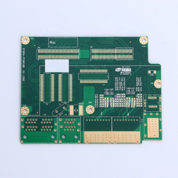
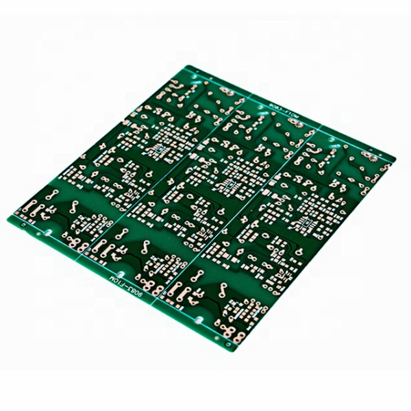
12v battery charger pcb 94vo printed circuit board
Basic Info
Model No.: Pcba Assembly and Part
Product Description
1. Reasons for PCB production:
1. EMC, for large-area ground or power supply copper, will play a shielding role, some special grounds, such as PGND play a protective role.
2. PCB process requirements, generally in order to ensure the effect of electroplating, or lamination is not deformed, copper is laid on the PCB layer with less wiring.
3. The signal integrity is required to provide a complete return path for the digital signal of the High frequency board and reduce the wiring of the DC network. Of course, there are also reasons such as heat dissipation, special device installation requires copper and so on.
2. The benefits of copper paving:
The biggest advantage of copper paving is to reduce the ground wire impedance (a large part of the so-called anti-interference is also caused by the reduction of ground wire impedance). There are a lot of spike currents in the Characteristic impedance PCB digital circuit, so it is more necessary to reduce the ground wire impedance. It is generally believed that a large area of ground should be laid for circuits composed of digital devices, while for analog circuits, the ground loop formed by laying copper will cause electromagnetic coupling interference to outweigh the gain (except for the High frequency board). Therefore, it is not that all circuits require ordinary copper (BTW: the performance of mesh copper paving is better than that of a whole block)
3. The significance of copper paving lies in:
1. Pave the copper and connect with the ground wire, so as to reduce the loop area
2. A large area of copper is equivalent to reducing the resistance of the ground wire and reducing the voltage drop. The digital ground and the analog ground should also be separated to lay the copper when the frequency is high, and then connected with a single point. The single point can be connected with a wire around a magnetic ring several times. However, if the frequency is not too high, or the working conditions of the instrument are not bad, it can be relatively relaxed. The crystal oscillator can be regarded as a high-frequency emission source in the circuit. You can spread copper around and ground the shell of the crystal oscillator, which will be better.
Fourth, the difference between the whole piece of copper and the grid:
To analyze specifically, there are about 3 functions:
1. Beautiful;
2. Suppress noise;
3. In order to reduce high-frequency interference (on High frequency board H), according to the wiring guidelines: the power supply and the ground layer should be as wide as possible, why do you need to add a grid? Isn't it inconsistent with the principle? From a high frequency point of view, it is even more wrong. The most taboo in the High frequency board wiring is the sharp traces. There are many problems with n 90 degrees in the power layer. In fact, why do it like that is entirely the requirement of the craft: see if the hand-soldered type is painted like that, almost none; if you see such a painting, there must be Surface-Mount (SMT) &BGA Assembly on it. At that time, because there was a process called Wave Solder for PCBA when mounting, he had to heat the PCB locally. If the copper is fully covered, the above specific heat coefficient is different, the board will be up and the board will be up, and then the problem will come. Under our current corrosion process: if the film is easy to stick to the PCB, in the subsequent strong acid project, that spot may not be corroded, and there are a lot of waste products! From this perspective, do you know why you have to paint like that? Of course, some surface mounts are not gridded. From the point of view of product consistency, there may be two situations: a. His corrosion process is very good; b. Instead of Wave Solder for PCBA, it is adopted. A more advanced reflow welding, but in this case, the investment of the entire assembly line will be 3-5 times higher.


Product Categories : High Frequency Board > Multi-wiring Printed Board

